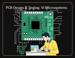
Over All Course Objective:
This course aims to equip students with the fundamental knowledge and practical skills required to design and develop single-layer and double-layer Printed Circuit Boards (PCBs) using KiCad software.
Students will gain hands-on experience in PCB fabrication using copper clad sheets, including image transfer and etching processes. The course also covers component assembly, soldering techniques, and final testing of the assembled PCB to ensure proper circuit functionality.
Learning Outcomes
Upon successful completion of this course, students will be able to:
- List the types and applications of PCBs in various industries.
- Identify common electronic components and their packaging types.
- Apply the PCB design workflow from schematic capture to fabrication and assembly.
- Apply design rules and standards for single and double-layer PCBs.
- Use KiCad tools effectively for schematic capture, PCB layout design, and footprint creation.
- Design and implement microcontroller-based circuits using KiCad.
- Employ optimal component placement strategies considering heat dissipation, signal integrity, and manufacturability.
- Implement proper routing techniques for single and double-layer PCBs while adhering to design rules and signal integrity considerations.
- Identify PCB design issues and troubleshoot them effectively.
- Generate Gerber files for PCB manufacturing.
- Fabricate single-sided PCBs using copper clad sheets, image transfer, drilling, and etching processes.
- Assemble and solder electronic components on fabricated PCBs.
- Perform testing and verification of assembled PCBs using appropriate measuring instruments.
- Identify faults in fabricated and assembled PCBs and carry out troubleshooting procedures.
- Apply best practices in PCB design, including Design for Manufacturability (DFM), thermal management, and documentation standards.
- Design and layout single or double-layer PCBs for specific electronic projects using KiCad tools.
- Create comprehensive PCB design documentation, including schematics, layout files, and Bill of Materials (BOM).
Main stream: Naan Mudhalvan
Sub stream: Polytechnic College
Language: English and Tamil
Course Outcomes: Design- Fabrication & Testing
Location: Tamil Nadu
Duration: 60 Hrs
System Requirements: Windows 10
Has subtitles: TRUE